Scanning tunneling
spectroscopy of In4Se3 layered semiconductor crystals
Chem.
Met. Alloys 4 (2011) 1-5
https://doi.org/10.30970/cma4.0135
P.V. GALIY, T.M. NENCHUK, O.R. DVERIY, A. CISZEWSKI, P. MAZUR, S. ZUBER, Ya.M. BUZHUK
The topography and local density of states of
the cleavage surfaces of a layered semiconductor In4Se3 (100)
crystal were analyzed by scanning tunneling microscopy (STM)
in situ. The shape and dimensions of
the acquired STM profiles correspond well to the bulk
lattice parameters. The local density of states and band gap for In4Se3 (100)
were obtained by scanning tunneling spectroscopy (STS), which gave the same gap
value as for the bulk crystal. The STM/STS results
show a local energetic and phase inhomogeneity of In4Se3 (100)
cleavage surfaces on the atomic scale. The studies confirm that the furrowed
and chainlike surface structure of In4Se3 (100) is
stable and unreconstructed under the cleavage and might be suitable as an
anisotropic, low-conductive matrix/template for fabrication of
surface-conductive nanowires or nanostructures.
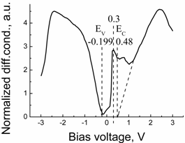
Typical averaged normalized STS
spectrum of n-type In4Se3
(100) UHV cleavage surface, acquired from 50x50 nm2
area. The
conduction and valence band edges are indicated by lines, and the ticmark at +0.3 V indicates a feature in the bandgap region that arises from localized states.
Keywords
Scanning tunneling spectroscopy / Scanning
tunneling microscopy / Local density of states / Low-dimensional structures /
Layered crystals / In4Se3