Surface microstructure and
optical properties of PbTe films on semiconductor and
dielectric substrates
Chem.
Met. Alloys 3
(2010) 140-146
https://doi.org/10.30970/cma3.0133
A.N. Harbachova, G.E. Malashkevich,
D.M. Freik, R.I. Nykyruy, G.P. Shevchenko
PbTe thin films on silicon, germanium, micaceous and glassy substrates, as well as on silica
substrates coated with SiO2-, GeO2-, and HfO2-gel
films, were prepared by means of precipitation from the gas-dynamical vapor
stream. The microstructure of the film surface and optical properties in the
middle IR-range as a function of the conditions of
preparation and the nature of the substrate were investigated by means of
scanning electron microscopy and FTIR spectroscopy.
Analysis of physical properties of the substrates allowed us to deduce a
correlation between the thermal conductivity of the substrate and
characteristics of PbTe films prepared under the same
conditions.
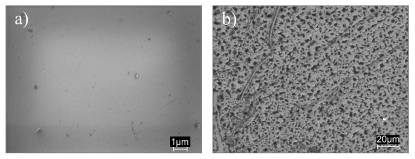
Scanning electron micrographs of PbTe films grown at Ts =
50°C, t = 15 min, on
silicon (a) and germanium (b) substrates.
Keywords
Surface microstructure / FTIR
spectroscopy / SEM / Thin films